Embedded Systems Part 2 - The Synchronous Duo I2C and SPI
[embedded-systems I2C and SPI are UART’s synchronous (and better) cousins and are the two most common protocols after UART.
Synchronous Communications
Unlike UART, SPI and I2C are both synchronous protocols, meaning that a clock signal is used to keep both the transmitter and receiver in sync during the data transfer. At every clock edge (either rising or falling), the transmitter knows to transmit data and the receiver knows to sample the data lines.
Synchronous communications are often much faster than asynchronous. For instance, I2C typically operates at around 100-400kHz and SPI can go to 10+MHz. This is due to the lack of overhead from start and stop bits and the presence of the clock signal means it’s a lot safer to send data faster without worrying about timing issues.
SPI
Let’s first look at SPI. Short for Serial Peripheral Interface, SPI is a protocol commonly used for communication between integrated circuits. Just like UART, SPI is full-duplex.
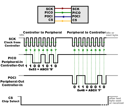
A typical SPI configuration is the Controller-Peripheral configuration. This configuration uses a total of four wires:
- SCK (Serial Clock, AKA the clock signal for syncing the transmitter and receiver)
- CS (Chip Select, an active low signal to address peripherals and start transmissions)
- POCI (Peripheral Out, Controller In, the data line that carries data from the peripheral to the controller)
- PICO (Peripheral In, Controller Out, the data line that carries data from the controller to the peripheral)
(Note: You may find some older sources that call Controller and Peripheral as Master and Slave respectively. These terms are problematic for obvious reasons. Newer naming conventions are in use but just know that regardless of the name, they refer to the same thing)
The naming of the wires makes it pretty straightforward to understand how SPI works. An SPI transaction starts when the controller pulls the CS signal low. This indicates to the peripheral that an SPI transmission is incoming. The clock signal using for pacing the data transfer is generated by the controller.
When data is sent from the controller to a peripheral, it’s sent on the PICO data line. If the peripheral needs to send data back to the controller, it’s sent on the POCI line. SPI data bits can be sent either MSB first or LSB first.
Clock Polarity and Clock Phase
SPI has four possible clocking configurations based on the clock polarity (CPOL) and clock phase (CPHA) that govern the way the clocking works.
CPOL represents the polarity of the clock. When set to 0, the clock is initially low (idles in the low state). When set to 1, the clock initially high (idles in the high state).
CPHA represents the phase of the clock. When set to 0, the first data bit is shifted out immediately when CS is pulled low. When set to 1, the first data bit is shifted out on the first clock edge after CS is pulled low.
With this, there are 4 possible SPI modes depending on the values of CPOL and CPHA:
- SPI Mode 0: CPOL = 0, CPHA = 0. Data is shifted out on a falling edge and the first bit is immediately shifted out when CS is pulled low. Data is sampled on a rising edge.
- SPI Mode 1: CPOL = 0, CPHA = 1. Data is shifted out on a rising edge and the first bit is shifted out on the first clock edge after CS is pulled low. Data is sampled on a falling edge.
- SPI Mode 2: CPOL = 1, CPHA = 0. Data is shifted out on a rising edge and the first bit is immediately shifted out when CS is pulled low. Data is sampled on a falling edge.
- SPI Mode 3: CPOL = 1, CPHA = 1. Data is shifted out on a rising edge and the first bit is shifted out on the first clock edge after CS is pulled low. Data is sampled on a rising edge.
Multiple Peripheral Configuration
SPI can support having multiple peripherals. These peripherals can be configured in either a Multiple Chip Select Configuration or Daisy Chain Configuration.
Multiple Chip Select is when each peripheral has its own unique CS line from the controller. This means that each peripheral can be individually addressed by pulling its respectively CS line low.
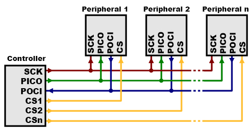
While convenient, this configuration can run into issues if you’re using a large number of peripherals as each of them require their own separate CS line. You can quickly run out of GPIO pins if this is the case.
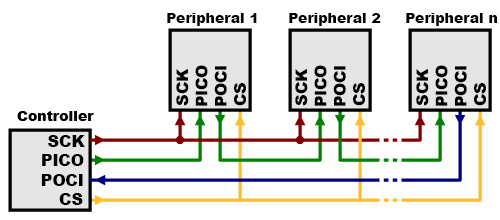
The Daisy Chain Configuration is when multiple peripherals share the same CS line. This means that when you pull the CS signal low, all of the peripherals are activated at once. This configuration may seem odd, but it’s useful in some cases such as using daisy-chained shift registers, addressable LED drivers, etc.
I2C
Now let’s look at I2C, short for Inter-Intergrated Circuit. Unlike SPI, I2C is a half-duplex synchronous communication protocol. As all devices in I2C share the same data line, data can only flow in one direction at a time.
There are a few more key differences between SPI and I2C:
- I2C only uses two wires.
- I2C can support having multiple controllers
- I2C has some overhead in the form of an ACK/NACK bit
- In a multiple peripheral configuration, the number of wires needed does not grow with the number of peripherals (i.e. it will always be two wires).
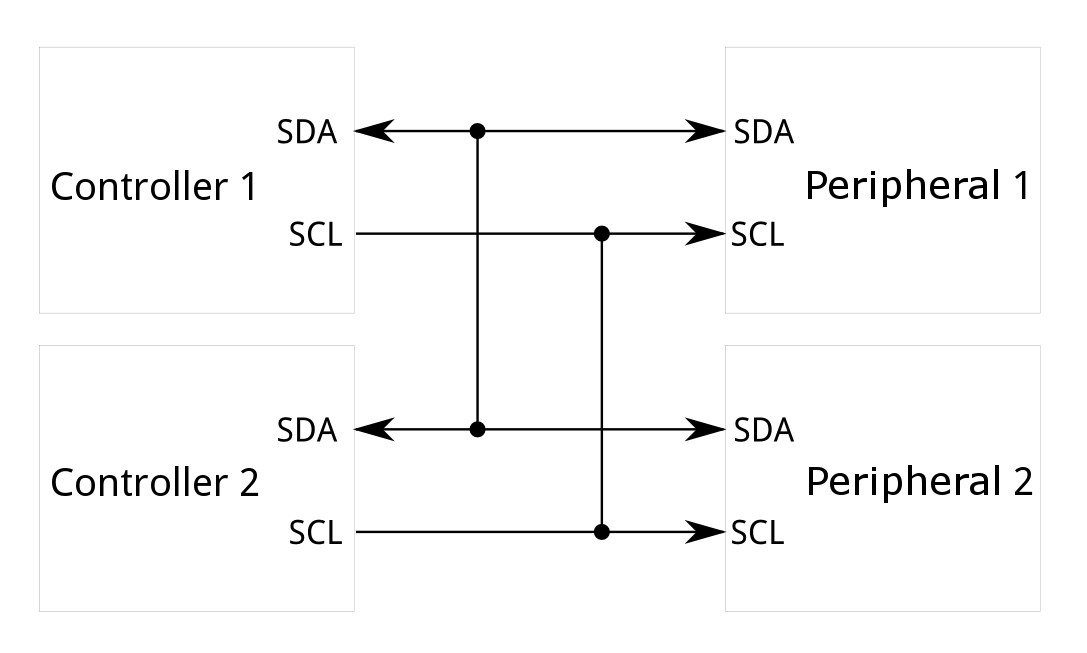
The two lines in I2C are known as SDA and SCL which stand for Serial Data and Serial Clock respectively. The clock signal is again, generated by the controller.
I2C lines are “open drain”. This means that the controller and peripheral can pull the lines low but cannot drive them high. This helps to eliminate ‘bus contention’ where one device may try to drive the line high while another tries to pull it low. The two I2C lines have pull-up resistors on them, to automatically keep the lines high when no device is pulling it low.
Communication
I2C communication is a bit more complex than UART and SPI and the signalling must adhere to the defined protocol for it to count as a valid transaction.
All I2C devices have their own addresses and each of them must have a unique address within the same system. This address is used to talk to the device involved in the transaction.
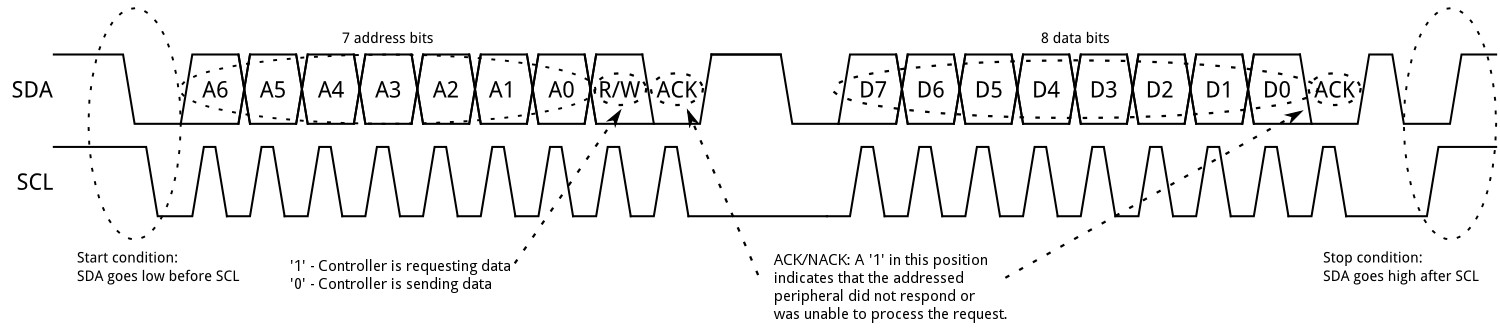
At the start of an I2C transaction, SDA transitions from high to low while SCL is high. This particular timing is important as this is how devices distinguish a start condition from regular data transmission. If there are two controllers, whichever pulls SDA low first takes control of the data lines.
Address Frame
The first transaction is the address frame. This frame contains the 7-bit I2C address that indicates which device that the transmission is meant for. All other devices that don’t have a matching address will know that the incoming data is not for them.
The address is shifted out MSB first and followed by a R/W bit. This indicates whether the transaction is a write or read operation (1 for read, 0 for write).
Once the address is transmitted, control of the SDA line is handed over to the receiving device during the 9th clock cycle (the ACK/NACK bit frame) for it to send an ACK bit by pulling the SDA line low to acknowledge the transmission.
If the receiver does not send an ACK bit, we can infer that the receiver did not get the message or the transmitted message was invalid. Remember that I2C devices cannot drive the line high, so no response automatically means a NACK bit. In the case of a NACK, this transaction is paused and it’s up to the controller to decide how to proceed.
Data Frames, Stopping and Repeated Starts
After the address frame is sent and acknowledged, data transmission begins. The controller generates clock pulses and the data is shifted out onto the SDA line by either the controller or peripheral, depending on whether it’s a read or write operation.
At the end of the data bits, the controller stops the transaction by releasing SCL (letting it go high via the pull-up) and then releases the SDA line, allowing it to also go high. It’s important to note that SCL must go high first before SDA. This also means that during data transmission, SDA must not change values when SCL is high to avoid a potential false stop.
In some cases, rather than ending a transaction with a stop, it is also possible to immediately start another transmission by sending another start condition (pulling SDA low and sending another address frame) before sending the stop condition. This is known as a repeated start. You can perform multiple repeated starts in a row. This is sometimes useful if you want to do a lot of read/write operations to the same device without releasing the bus, ensuring that the controller does not get interrupted. In this case, the stop condition condition only occurs at the very end of the repeated starts.
Other I2C Concepts
10-bit addresses
Some I2C devices may have 10-bit long addresses rather than 7-bits, requiring two address frames to transmit the address. The first frame consists of the bit sequence ‘b11110xyz’ where ‘x’ is the MSB of the address, ‘y’ is the 2nd MSB of the address’ and ‘z’ is the R/W bit.
The first frame will be acknowledged by devices that have the same first two bits as ‘x’ and ‘y’. The second frame then transmits the rest of the address to indicate the device. Using 10 bits increases the number of unique I2C addresses, preventing potential conflicts.
Clock Stretching
When a controller is sending or reading data faster than a peripheral can handle, usually due to it being busy with other operations, the peripheral can hold on the SCL line low until it is free to handle the I2C transaction again.