Embedded Systems Part 4 - Interacting with the Analog World
[embedded-systems Embedded systems are digital. However, the world around us is not made of 1’s and 0’s. The world we live in is analog. The things we perceive are analog. So no matter how advanced processors can get, they will always need an interface to bridge the gap between the analog world and the digital domain. These interfaces are known as Digital-to-Analog Converters (DACs) and Analog-to-Digital Converters (ADCs).
DACs
DACs convert a sequence of bits to an analog voltage. It takes the binary number and convert it to a voltage that is proportional to the binary number. By feeding a DAC with many binary numbers in quick succession we can generate an analog waveform.
The longer the binary number, the higher the resolution of the DAC. This is because more bits translate to more possible output values and hence smaller step sizes with each increment of the binary number. An n-bit DAC will have 2n possible outputs. So for example, an 4-bit DAC will have 24 or 16 possible outputs.
In practice, the input binary bits are generated using some sort of digital circuit or microcontroller.
The range of the output voltage is determined by Vref or the reference voltage of the DAC. Vref is generally the logic HIGH voltage of the MCU, which is usually 3.3V or 5V. So for a 3.3V logic level, the DAC output is between 0V to 3.3V.
The full-scale voltage VFS of a DAC is the maximum output voltage, which is achieved when the largest binary number is applied. For a 4-bit DAC, this number is 1111. In general:
\[V_{FS} = (\frac{2^n - 1}{2^n} \times V_{ref})\]So assuming a Vref of 3.3V, the maximum output voltage is about 3.09V.
Types of DACs
There are many, many types of DACs out there and to keep this post short and simple, I’ll only talk about two common types of DACs (there’s plenty of material online if you’d like to learn more).
Binary-weighted DAC
First is the binary-weighted DAC.
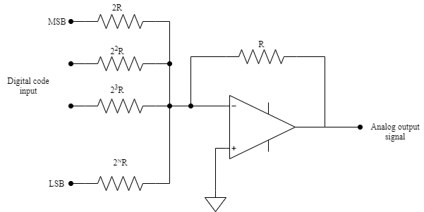
The binary-weighted DAC makes clever use of a summing amplifier to perform the digital to analog conversion. Recall that the output voltage of a summing amplifier is given by:
\[V_{out} = -(\frac{R_F}{R_1} \times V_{1} + \frac{R_F}{R_2} \times V_{2} + .... \frac{R_F}{R_n} \times V_{n})\]where n is the number of inputs to the summing amplifier and Vn is the input voltage at each bit (n = 1 is the MSB).
Each digit in the binary number is given a different weightage for their contributions to the output analog voltage. The weightages increase in powers of 2, hence the name binary-weighted.
By plugging in the resistances into the summing amplifier formula, we can see that the most significant bit (MSB) being the highest valued digit, has the highest weightage and the least significant bit (LSB) has the lowest weightage.
With reference to the above diagram, assume we have a 4-bit binary-weighted DAC, the binary input is 1010 and R = 1kΩ. Let’s also assume that the logic level voltage is 3.3V. So a ‘1’ will represent an input voltage of 3.3V and a ‘0’ will represent an input voltage of 0V. The output is therefore:
\[V_{out} = -(\frac{1k\Omega}{2k\Omega} \times 3.3V + \frac{1k\Omega}{4k\Omega} \times 0V + \frac{1k\Omega}{8k\Omega} \times 3.3V + \frac{1k\Omega}{16k\Omega} \times 0V)\] \[V_{out} = - (1.65V + 0V + 0.4125V + 0V) = -2.0625V\]The binary-weighted DAC is a simple and straightforward design. However, it is actually not so practical as it would require using a large range of resistors with very low tolerances (one for each bit) to obtain an accurate result. This would get expensive real quick for a higher resolution DAC (imagine needing to get 16 different precision resistor values for a 16 bit DAC).
R-2R Ladder DAC
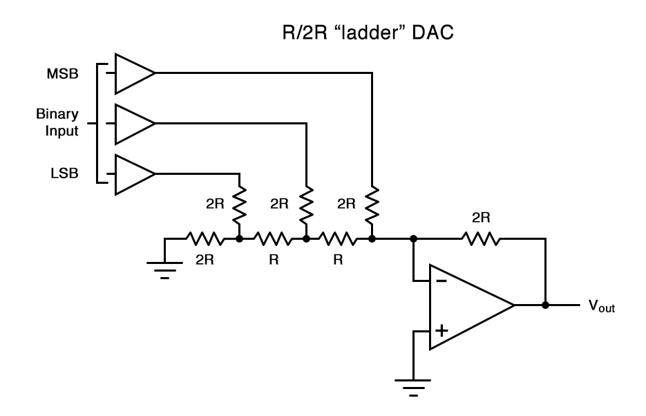
The R-2R Ladder DAC as its name implies, uses a ladder-like network of resistors to convert digital voltages to analog. As we can see, the R-2R Ladder DAC only needs two resistor values (R and 2R) which makes it much easier to achieve a good level of accuracy.
The output voltage is given by:
\[V_{out} = \frac{2^{0} \times V_{1} + 2^{1} \times V_{2} + ... \ 2^{n-1} \times V_{n}} {2^n}\]where n is the number of inputs to the summing amplifier and Vn is the input voltage at each bit (n = 1 is the LSB).
Due to my laziness, I won’t show how to derive the equation for the output voltage, but if you’d like, you can try to derive it by combining the series and parallel resistors to find the proportional voltage values being contributed to the final analog voltage by each bit.
Using the same assumptions for the binary-weighted DAC, we can calculate the output voltage as such:
\[V_{out} = \frac{1 \times 0V + 2 \times 3.3V + 4 \times 0V + 8 \times 3.3V }{2^4}\] \[V_{out} = \frac{6.6V + 26.4V}{16} = 2.0625V\]We get the same value as the binary-weighted DAC (only not inverted).
ADCs
The inverse of a DAC is an ADC. ADCs basically takes snapshots of an analog voltage at a point in time and uses these snapshots to produce a binary number that represents this analog voltage.
The basic ideas of DACs generally apply to ADCs as well. Their resolution is defined by the number of bits and the ADC can only accept inputs with a voltage range between Vref and 0V.
Types of ADCs
Just as with DACs, we won’t be talking exhaustively about all the various types of ADCs out there. Here, we’ll only be talking about one type of ADC - The Successive Approximation Register (SAR) ADC.
The SAR ADC is arguably the most popular ADC architecture out there thanks to its small form factor and low power demands. Barring certain applications that require extremely fast sampling rates, SAR ADCs are basically everywhere.
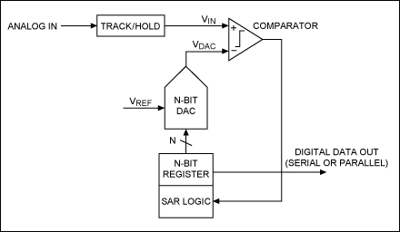
There are many possible variations for implement a SAR ADC, however the basic architecture is generally the same, consisting of a comparator, a sample-and-hold circuit and a DAC. That’s right, a SAR ADC has a DAC inside of it.
As you may guess from its name, a SAR ADC converts analog voltage into binary by making approximations in rapid succession. The algorithm flows as such:
-
The DAC output is set to half of Vref by setting the MSB of the register to 1.
-
The output of the DAC is fed to the comparator, that compares the DAC voltage with the input voltage. If the input is voltage is higher than the DAC voltage, then the comparator output is a logic HIGH and the MSB remains at 1. Otherwise the MSB is set to 0.
-
We then move to the next bit and set it to 1 (so the register value at this point could either be 01… or 10…. depending on the result of step 2). Once again, we compare the DAC voltage with the input voltage and again we set the bit to 1 is the input voltage is higher or 0 if the input voltage is lower.
-
Repeat the operations from steps 1 to 3 for all bits in the register. With each comparison, the register value converges on the binary representation of the input voltage.
Notice that we need N number of comparisons for an N-bit SAR ADC. This means that there is an inherent trade-off between speed and resolution. if you want a higher resolution, then the speed would have to go down and vice versa. You can find SAR ADCs that go up to 24 bits of resolution, but their speed is limited to a few megasamples/second and conversely you’ll find SAR ADCs with speeds of tens of megasamples/second but their resolution is lower.
This relationship between speed and resolution tends to hold for other ADC architectures as well. For example, the fastest ADCs are Flash ADCs. They have a large bank of comparators and amplifiers to rapidly convert analog voltages to digital values at speeds in the gigasamples/second range. However, a Flash ADC’s resolution generally goes up to 10 bits at most, as for every bit of resolution you add you’d increase the number of comparators by a factor of 2, which quickly makes it not a feasible design.
On the other end of the spectrum, Sigma-Delta ADCs can attain very high resolutions up to 32 bits, but their speed can really only go up to 1 megasample/second.